1

Comments

Long time no see. I bought an Ar.Drone2 and try to do some development about it's hardware. However, on its website, it only tell us the function about the component but not the type of the component. So I decided to disassemble it and figure out what's on the drone's PCB.

After taking out drone's shell, I can see 2 PCB. The big one is motherboard, another small one is sensors board. The 3 axis gyroscope, 3 axis accelerometer and 3 axis magnetometer and a pressure sensor is one the sensor's board, and the ultrasonic sensors is also connected to this small board. There is also a PIC MCU on the small board to manage all the sensor and connect to the big motherboard.
PCB1

There has so many component on the motherboard. 2 video cameras are connected one the bottom side of the motherboard. On the top side of the motherboard, there has 2 connector to connect the 4 motors. One connector is power supply, another one is signal line. There is an Qualcomm's AR6103 802.11 b/g/n Wifi Radio Chip which use to connect the Android phone or iPhone or iPad.

After taking out the shied, I can see 3 chips. Ti's TPS65921, Micron's MT46H32M32LFMA-5 IT with FBGA code: D9MBZ, a 200MHz 128M RAM and Micron's MT29F1G08ABBDAH4-IT with FBGA code: NQ278, an 1G SLC ECC NAND flash. But I can't see the CPU because the CPU is under the RAM by using the "Package on package" PoP-FCBGA package type just like the Raspberry Pi. Considerate the electronic assistance specification which published on the Ar.Drone's website that the CPU is 1GHz ARM® Cortex™ A8 + 800 MHz DSP TMS320C64+™ core and the frequents of the CPU, the footprint of the PoP RAM and the TI's power manage scheme, I can figure out that the CPU may be the TI's DM3730, Digital Media Processors.

PCB2

2

Comments

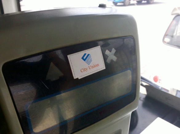
7 月 15 日左右, 兰州, 白银, 上海, 湖州, 绍兴, 宁波, 台州公交卡可以互通. 7 月 18 日, 我成功地在宁波公交 503 线上使用上海公交卡支付了车费. 根据"全国城市一卡通互联互通"也就是City Union规范, 在未来几年间, 将更多城市融入互通系统.
一辆公交车上的City Union标志

互通面临的问题: 硬件 算法 结算

硬件: 由于在各个城市的非接触式公交卡发行的时候, 并没有采用相同公司的产品. 各个公司为了专利可能生产不同规范产品. 他们可能是频率不同, 或者握手信号时许不同. City Union 采用了 ISO 14443 的规范. 个别城市的设备采用了私有规范, 卡片从物理角度上就不遵循这个规范, 因此该卡片无法接收规范化终端的信号, 也就不能用于互通. 这就导致该城市市民必须购买新卡片才能用于其他城市, 如杭州. 更有可能为了兼容城市私有卡片和互通卡片, 更换所有的刷卡机.

算法: 每一张卡片上有一定大小的 ROM 用来存储数据. 在终端如刷卡机, 地铁匝机上消费时, 终端将卡片 ROM 上的信息读取, 解码, 然后结算, 加密, 重新写入卡片 ROM. 但是每个城市的加密算法可能不同, 这将导致异地消费时卡片数据可以读取, 但无法解码. 这样的城市只要重新修改刷卡机软件算法就可以了. 对于卡片, 则需要到充值网点升级内部数据而不需要另外掏钱.

结算: 由于公交卡是预付费的, 当拿 A 城市的卡用于 B 城市的交通系统时, A 城市收了钱而 B 城市白白载客了. 另外各个城市的卡片优惠也不同. 如宁波对于本地预付费的卡片的折扣为 6 折, 而我使用上海公交卡时, 却没有任何折扣. 其实, 没有收我漫游费我已经很开心了.

< ,>
1

Comments

<- 左箭头:数据向右移动一位(光标向左移动一位) logic shift right 1 bit, cursor shift left 1 bit
-> 右箭头:数据向左移动一位(光标向右移动一位) logic shift left 1 bit, cursor shift right 1 bit
1:将当前光标所在位置1 set the cursor bit as 1
0:将当前光标所在位置1 set the cursor bit as 0

a number w/ a box and up/down arrow 数字,带有框和上下方向的箭头: 如果光标所在位是框内的数字, 转移到箭头向上/下的语句, 否则继续前进. 如果框内没有数字, 表明转移条件是这个位是空白的.If the cursor bit is the number in the box, jump into arrow up/down, else go ahead. The blank box means this the branch condition is if this bit is blank.

a loop arrow w/ some bits inside: 一个环箭头, 里面有一些点: 回到前面. 几个点表示回到几个指令之前. Loop back, the amount of the small bit inside means how many instructions should loop back.

e.g(RED for cursor) The first puzzle in google doodle.
00010 -> 01011

So let's do this.

_LSR 00010 -> 00010
SET1 00010 -> 01010 //We must change the operator "0" into "1".
_LSL 01010 -> 01010
_LSL 01010 -> 01010
_LSL 01010 -> 01010
SET1 01010 -> 01011 //We must change the operator "0" into "1".

Got it! Like basic assembly language?
Have fun w/ this amazing machine. Hail to Alan Mathison Turing, an mathematician, logician, cryptanalyst and computer scientist.

< >
1

Comments

Long day for me to update my blog. I even don't know my blog was blocked by our Great Fire Wall.

Yesterday I passed my first time of GRE test. That's a f**k test. But during the day of preparing the GRE, I got a chance to attend our University's electronic design contest. In the contest, I fixed some problems of my power and add some now function into it.


This is the top layer of the power. You can see a black PCB which plug into the main board. That's a current detection module. I using TI's INA200A to detecting the current of power's output. Then using Arduino's ADC to check out the current if the current exceeds the threshold value. This threshold value could change during the runtime. If the power is overloaded, the relay (yellow thing) will cut off the output to protect the buck chip until manual reset the system.

The 1602 LCD could display the output voltage, output current and cut off thrshold current value. Using Arduino to control the LCD is very simple like using printf() function in C language.


This the bottom layer of the power. I using the surface mount package part to keep the system small.


This is the out put waveforms. About 15mV ripple voltage in 1A load, 10V output. Fantastic result by using Nichicon HD aluminium electrolytic capacitor.

That's all of the
This project is open-sourced, under the licence of BY-NC-SA. If you want the SCH, PCB file and Arduino file, leave the comment and I will mail you ASAP.
Thanks to Texas Instruments for offering me so many kind of chips free.

< ,,>
0

Comments

We use TI's TLC5615, 10-BIT DIGITAL-TO-ANALOG CONVERTERS as our DAC.
This chip has 3-Wire Serial Interface, so we can use Arduino to control it.
Arduino is an open-source physical computing platform based on the AVR MCU.
Now give the Arduino program.

//Arduino project http://arduino.cc
//by Mini Dragon at http://minidr.com/archives/687
//This program is licensed under a Creative Commons Attribution-ShareAlike 3.0 License.
#define CS 2 //chip enable
#define CLOCK 3
#define DATA  4
 
#define HALF_CLOCK_PERIOD 2 //2 uS of clock period 
float j=0;
void setup()
{
	pinMode(DATA, OUTPUT);
	pinMode(CLOCK,OUTPUT);
	pinMode(CS,OUTPUT);
	digitalWrite(CS,HIGH);
	digitalWrite(DATA,LOW);
	digitalWrite(CLOCK,LOW); 
}
 
void writeValue(uint16_t value)
{
	digitalWrite(CS,LOW);//start of 12 bit data sequence
	digitalWrite(CLOCK,LOW);
	data = data << 2; //Add 2 0 at the end of the data. A 10-bit data word should add 2 0 at the LSB bit (sub-LSB) since the DAC input latch is 12 bits wide.(SEE TLC5615C DATASHEET) 	
	for(int i=11; i>=0; i--)//send the 12 bit sample data
	{
		digitalWrite(DATA, (value & (1 << i) ) >> i );//DATA ready
		delayMicroseconds(HALF_CLOCK_PERIOD);
		digitalWrite(CLOCK,HIGH);//DAC get DATA at positive edge
		delayMicroseconds(HALF_CLOCK_PERIOD);
		digitalWrite(CLOCK,LOW);
	}
	digitalWrite(CS,HIGH);//end 12 bit data sequence
}
 
void loop()
{
	j=567; //in here, 567 is a example. DAC OUT=j*Vref/1024
	writeValue(floor(j));
}

Each DAC output voltage maps a main Vout.
To be continued.

[Update 2014/Tue/22] Code Opt

< ,,>
21

Comments

I just explored an easy scheme to design a high precision programmed adjustable power.
In this scheme, there is no needs to make a complex PWM circult, just a liner or switcher adjustable voltage regulator and a resister network, a DAC, and a MCU. Resister network change DAC output voltage into feedback voltage and let adjustable voltage regulator regulate output voltage itself.

Outputting an fixed voltage by using resister to control regulator may be easy, but there is a little challenge to output adjustable voltage. My mates used to use digital potentiometer to adjust output voltage, but digital potentiometer is too instable. Lucky, DAC with a resister network works better, and they can provide high precision output witch depends the resolution of DAC.

fig1

In this figure, voltage of the node feedback is fixed by the Vref (OR Vsense) of regulator.LM2576 is 1.23V, TPS5432 is 0.808V.
When there is voltage difference between Vout of DAC and Vref of regulator, the difference sets up an current in R2. Then the current through R1 to the ground. This adjustable current could change the resistance because voltage between Vref and GND is fixed and no current will go into Vref pin duo to the virtual short and virtual open of the error amplifier inside of the regulator chip.
Now it's time to value R3, R2, R1. Make sure that the output range of this regulator (Vout) and DAC (Vdac) , and Vref by checking the datasheet of part.
Then, list two equation.

(Vdac.max-Vref)/R2+(Vout.min-Vref)/R3=Vref/R1
(Vdac.min-Vref)/R2+(Vout.max-Vref)/R3=Vref/R1

Three unknown resistance, but two equation, we must assume the value of R3. 10K is very common.
Then check the Idac.max to make sure that DAC will not overloaded.

[Update 2014/Tue/22] PS: Three terminal regulator, such as LM317 is not available to this equation because the 1.25V is between Ref pin and out pin.

To be continued.

< >