Long time no see. I bought an Ar.Drone2 and try to do some development about it's hardware. However, on its website, it only tell us the function about the component but not the type of the component. So I decided to disassemble it and figure out what's on the drone's PCB.
After taking out drone's shell, I can see 2 PCB. The big one is motherboard, another small one is sensors board. The 3 axis gyroscope, 3 axis accelerometer and 3 axis magnetometer and a pressure sensor is one the sensor's board, and the ultrasonic sensors is also connected to this small board. There is also a PIC MCU on the small board to manage all the sensor and connect to the big motherboard.

There has so many component on the motherboard. 2 video cameras are connected one the bottom side of the motherboard. On the top side of the motherboard, there has 2 connector to connect the 4 motors. One connector is power supply, another one is signal line. There is an Qualcomm's AR6103 802.11 b/g/n Wifi Radio Chip which use to connect the Android phone or iPhone or iPad.
After taking out the shied, I can see 3 chips. Ti's TPS65921, Micron's MT46H32M32LFMA-5 IT with FBGA code: D9MBZ, a 200MHz 128M RAM and Micron's MT29F1G08ABBDAH4-IT with FBGA code: NQ278, an 1G SLC ECC NAND flash. But I can't see the CPU because the CPU is under the RAM by using the "Package on package" PoP-FCBGA package type just like the Raspberry Pi. Considerate the electronic assistance specification which published on the Ar.Drone's website that the CPU is 1GHz ARM® Cortex™ A8 + 800 MHz DSP TMS320C64+™ core and the frequents of the CPU, the footprint of the PoP RAM and the TI's power manage scheme, I can figure out that the CPU may be the TI's DM3730, Digital Media Processors.

Long day for me to update my blog. I even don't know my blog was blocked by our Great Fire Wall.
Yesterday I passed my first time of GRE test. That's a f**k test. But during the day of preparing the GRE, I got a chance to attend our University's electronic design contest. In the contest, I fixed some problems of my power and add some now function into it.

This is the top layer of the power. You can see a black PCB which plug into the main board. That's a current detection module. I using TI's INA200A to detecting the current of power's output. Then using Arduino's ADC to check out the current if the current exceeds the threshold value. This threshold value could change during the runtime. If the power is overloaded, the relay (yellow thing) will cut off the output to protect the buck chip until manual reset the system.
The 1602 LCD could display the output voltage, output current and cut off thrshold current value. Using Arduino to control the LCD is very simple like using printf() function in C language.

This the bottom layer of the power. I using the surface mount package part to keep the system small.

This is the out put waveforms. About 15mV ripple voltage in 1A load, 10V output. Fantastic result by using Nichicon HD aluminium electrolytic capacitor.
That's all of the
This project is open-sourced, under the licence of BY-NC-SA. If you want the SCH, PCB file and Arduino file, leave the comment and I will mail you ASAP.
Thanks to Texas Instruments for offering me so many kind of chips free.
< arduino,DAC,power >
We use TI's TLC5615, 10-BIT DIGITAL-TO-ANALOG CONVERTERS as our DAC.
This chip has 3-Wire Serial Interface, so we can use Arduino to control it.
Arduino is an open-source physical computing platform based on the AVR MCU.
Now give the Arduino program.
//Arduino project http://arduino.cc
//by Mini Dragon at http://minidr.com/archives/687
//This program is licensed under a Creative Commons Attribution-ShareAlike 3.0 License.
#define CS 2 //chip enable
#define CLOCK 3
#define DATA  4

#define HALF_CLOCK_PERIOD 2 //2 uS of clock period
float j=0;
void setup()
{
	pinMode(DATA, OUTPUT);
	pinMode(CLOCK,OUTPUT);
	pinMode(CS,OUTPUT);
	digitalWrite(CS,HIGH);
	digitalWrite(DATA,LOW);
	digitalWrite(CLOCK,LOW);
}

void writeValue(uint16_t value)
{
	digitalWrite(CS,LOW);//start of 12 bit data sequence
	digitalWrite(CLOCK,LOW);
	data = data << 2; //Add 2 0 at the end of the data. A 10-bit data word should add 2 0 at the LSB bit (sub-LSB) since the DAC input latch is 12 bits wide.(SEE TLC5615C DATASHEET)
	for(int i=11; i>=0; i--)//send the 12 bit sample data
	{
		digitalWrite(DATA, (value & (1 << i) ) >> i );//DATA ready
		delayMicroseconds(HALF_CLOCK_PERIOD);
		digitalWrite(CLOCK,HIGH);//DAC get DATA at positive edge
		delayMicroseconds(HALF_CLOCK_PERIOD);
		digitalWrite(CLOCK,LOW);
	}
	digitalWrite(CS,HIGH);//end 12 bit data sequence
}

void loop()
{
	j=567; //in here, 567 is a example. DAC OUT=j*Vref/1024
	writeValue(floor(j));
} |
Each DAC output voltage maps a main Vout.
To be continued.
[Update 2014/Tue/22] Code Opt
< arduino,DAC,TLC5615 >
I just explored an easy scheme to design a high precision programmed adjustable power.
In this scheme, there is no needs to make a complex PWM circult, just a liner or switcher adjustable voltage regulator and a resister network, a DAC, and a MCU. Resister network change DAC output voltage into feedback voltage and let adjustable voltage regulator regulate output voltage itself.
Outputting an fixed voltage by using resister to control regulator may be easy, but there is a little challenge to output adjustable voltage. My mates used to use digital potentiometer to adjust output voltage, but digital potentiometer is too instable. Lucky, DAC with a resister network works better, and they can provide high precision output witch depends the resolution of DAC.

In this figure, voltage of the node feedback is fixed by the Vref (OR Vsense) of regulator.LM2576 is 1.23V, TPS5432 is 0.808V.
When there is voltage difference between Vout of DAC and Vref of regulator, the difference sets up an current in R2. Then the current through R1 to the ground. This adjustable current could change the resistance because voltage between Vref and GND is fixed and no current will go into Vref pin duo to the virtual short and virtual open of the error amplifier inside of the regulator chip.
Now it's time to value R3, R2, R1. Make sure that the output range of this regulator (Vout) and DAC (Vdac) , and Vref by checking the datasheet of part.
Then, list two equation.
(Vdac.max-Vref)/R2+(Vout.min-Vref)/R3=Vref/R1
(Vdac.min-Vref)/R2+(Vout.max-Vref)/R3=Vref/R1
Three unknown resistance, but two equation, we must assume the value of R3. 10K is very common.
Then check the Idac.max to make sure that DAC will not overloaded.
[Update 2014/Tue/22] PS: Three terminal regulator, such as LM317 is not available to this equation because the 1.25V is between Ref pin and out pin.
To be continued.
< power >
伟大的电子设计产物, 电源组竞赛作品样品, 400V 高压 PFC 直流输入, 反激 + TL431 反馈, 36V 2A 输出, 设计优良的 "大只" 电源, 因制作新电源缺乏材料, 于 2011 年 12 月 17 日上午 8 点 30 分被拆解.
"大只" 电源是 TOP Switch 系列电源的伟大领导者, 它把毕生精力献给了繁荣开关电源的伟大事业, 建立了不朽的历史功勋. "大只" 电源是电子设计参赛同学的亲密朋友, 它以极大热情继承和发展了同学对电子设计的乐趣, 同老师同学结下了深厚友谊, 有力地推动了鄙校电子设计不断向前发展. 全体电子设计同学对 "大只" 电源的逝世深感悲痛, 我们将永远怀念它.


根据 信息时报 的报道, 爱疯"只要一不符合保修条件, 就需要支付上千元甚至与手机价格相近的维修费用".
前几天我们工作室里的一个同学要我来帮他会诊下他的 touch. 他的 touch 无法开机, 充电无显示, 送修, 被告知要换主板, 需要支付一千多的费用.
同学觉得有点坑爹. 于是没有修, 拿过来帮我会诊.
我拿到手后拆开, 检查了一下是电池没有电压输出. 用外部电源接到电源接口发现机器能工作. 判断电池损坏.
然后查了下是电池短路, 请隔壁寝室同学解锁解锁, 稍微充了一点电. 能正常开机, 就是无法充电.
后来仔细一检查是机身尾部的排插口中的电源针断了, 用引线拉出能正常充电.
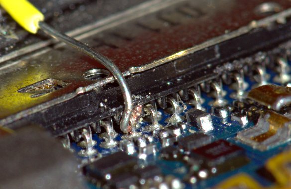
因为主板上插座附近元件焊点比较多, 不敢从淘宝上买一个 (25软妹币) 自己焊接, 然后拿到学校边上的小店指明就换那个插件, 价格就少很多了.
技术宅拯救世界啊~!
< 苹果 >
Comments